While investment in the technology sector as a whole has plunged during the last two years, research and development into semiconductor technology – some of which will not see the light of day for decades – is gathering pace.
It certainly needs to if computer power is to continue increasing in accordance with Moore's Law – the observation of the Intel co-founder that the number of transistors on a chip doubles approximately every 18 months, enabling a doubling of speed and power.
Carried to its logical conclusion, Moore's Law suggests that by 2007, microprocessors should be designed in 0.045 micron process geometry, compared to the 0.13 and 0.18 used today, with typical PCs operating at about one terahertz (THz).
Yet at the same time, analysts argue that current materials such as copper and silicon will soon be unable to go any faster. That is why researchers are examining a whole range of techniques and technologies to wring still more performance out of the computers of the future.
The question is, which technologies are ready – or almost ready – to leap out of the laboratory, and which will remain a distant pipedream, pursued by cranks, dreamers, academics and the terminally over-optimistic? Infoconomist looks at the key contenders.
Terahertz transistors
Funding
Microelectromechanical system (MEMS) motors
Companies to watch:
Spherical Semiconductors
Ovonics
Plastics
Nanotechnology
Notable breakthroughs
Terahertz transistors
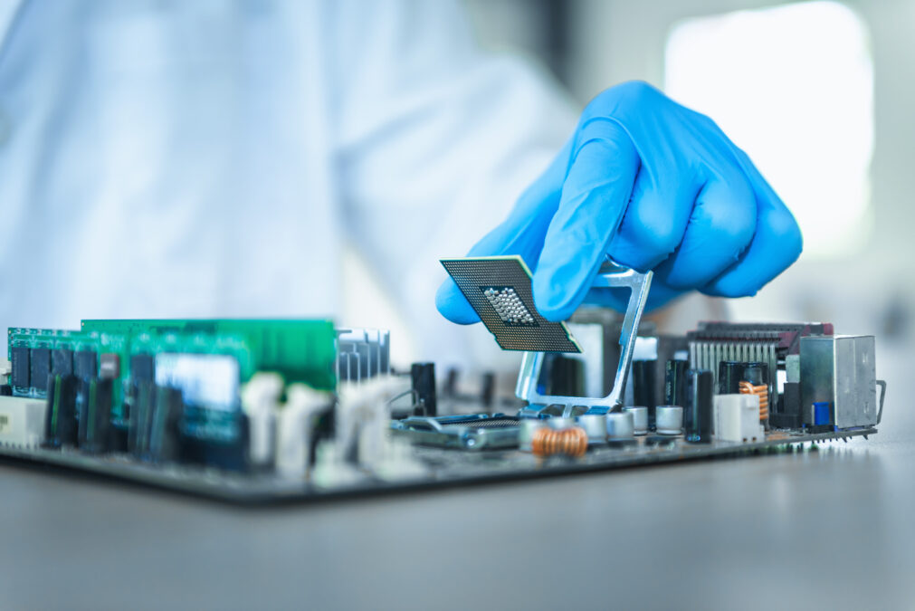
Transistors are the main building blocks of microprocessors – the more of them on a chip, and the faster they can go, the better. That is why Advanced Micro Devices (AMD), IBM and Intel have been crowing about ‘terahertz transistors'.
In December 2001, AMD announced that it had developed a transistor capable of running at 3,300 gigahertz (GHz) – or 3.3 terahertz (THz). AMD achieved this on an experimental 0.015 micron process transistor which, it says, will help it make microprocessors ten time more powerful than its current fastest chip.
Unfortunately, AMD's VP of technology development Craig Sander does not expect the innovation to appear commercially before the end of the decade, but companies such as AMD are keen to publicise such breakthroughs in a bid to demonstrate that they will be able to keep up with Moore's Law for the foreseeable future.
Indeed, at the same trade show that AMD unveiled its research, IBM unveiled what it called its ‘double gate' transistor design. According to IBM, as microprocessors get smaller and smaller, traditional transistor gates, which can be set to either on or off, have a tendency to leak electricity, even when they are supposed to be off.
IBM says that using two gates doubles the control of the current and will enable even smaller, faster and lower power circuits to be designed. Intel, of course, is also in the game. In contrast to IBM, it has been experimenting with new materials that could potentially replace Silicon Dioxide. Intel engineers believe that Zirconium Dioxide provides superior insulation and is, therefore, a far better material for building the transistor gates.
Back
Funding
Ever since the invention of the transistor, semiconductor technology has proved to be an almost never-ending source of innovation. However, much of the most exciting research in MEMS, nanotechnology and plastics is being conducted either by deep-pocketed organisations, such as Intel, IBM and Philips, or by academic institutions.
The one venture fund that has been keen to invest in these new areas has been Intel Capital – the VC arm of the semiconductor giant. However, many other VC funds are now looking more closely at these areas.
Back
Microelectromechanical system (MEMS) motors
As semiconductor equipment makers have been able to shrink the width of the circuitry within microprocessors and memory chips, so some researchers have been turning their attention to making sophisticated microscopic machines using similar technology.
Companies such as Intel are now taking advantage of process widths of just 0.13 microns. But in January 2002, the US Department of Energy's Sandia National Laboratory demonstrated a ‘microchain drive' of little more than 50 microns wide – less than the width of a single human hair.
Sandia technician Ed Vernon says that MEMS could be used to help miniaturise devices that currently use bigger and clunkier mechanicals. For example, they could be used in camera shutters. It is not just government funded ‘blue sky' researchers that have been examining the potential of MEMS. Semiconductor giants such as Texas Instruments and Intel are also investing time and money because of the complimentary way in which MEMS could potentially be adopted in the computer industry.
For example, Intel believes that MEMS could be used to help network computers through laser beams and rotating mirrors, instead of cabling.
The company is also looking at how it could design MEMS technology to utilise the heat dissipated by microprocessors to drive other processes in a computer.
Back
- Ball Semiconductor – US – Ovonics
- E-Ink – US – Plastics
- Plastic Logic – UK – Plastics
- Zyvex – US – Nanotechnology
Intel has invested in at least six MEMS start-ups.
Back
Spherical Semiconductors
When Akira Ishikawa and Hideshi Nakano founded Ball Semiconductor in 1996, they might have been dismissed as mad were it not for their lengthy and distinguished backgrounds in the semiconductor industry.
Ishikawa's idea was simple. Instead of building integrated circuits on flat wafers, why not do it on balls? Furthermore, instead of fabricating semiconductors in expensive ‘clean rooms', why not do so in sealed tubes and pipes?
Ishikawa believes that this process could potentially cut the cost of making microprocessors by 90%. The company can boast some success, including building its own working fabrication facilities, with which is has fabricated transistors with characteristics similar to those found on a standard semiconductor.
But there is little evidence that the rest of the industry is preparing to adapt to Ball Semiconductor's technology and, as a result, the company is focusing on the microelectromechanical system (MEMS) motor market, rather than the mainstream chip market.
Back
Ovonics
Although Intel was forced to withdraw from the commodity memory market in 1984, it has never had to make such an ignominious retreat from flash memory – a form of memory that requires little electricity to retain its state and that is, therefore, widely used in mobile devices.
In February 2002, the company announced a new technology called ovonics, which may enable it to forge further ahead in this area.
Although ovonics has been applied to nickel-hydride batteries and re-writeable CDs, Intel is the first to use it in memory. Ovonics is a method of changing amorphous substances into a crystalline state. It can be used to generate binary code and, thereby, to read and write data faster than standard flash memory.
Furthermore, ovonics offers the possibility of more reliable and longer-lasting memory chips. A standard flash memory chip can be written over around a million times, but data can be written to ovonic memory more than a trillion times, according to Intel researchers.
As a result, Intel forecasts that ovonic memory could become widespread in mobile phones and other devices within five years.
Back
Plastics
Quite how researchers alighted on the idea of using plastics in semiconductors is something of a mystery: conventionally, plastic does not conduct electricity, hence its widespread use as a packaging material in the electronics industry.
But in recent years, scientists at five separate organisations have demonstrated new plastic substances that can offer many of the conductive properties of traditional semiconductor material. The new technology is based on research into polymers called olythiophenes and oligothiophenes.
Traditional semiconductor technology requires eight or 12-inch silicon wafers to be repeatedly etched using lasor lithography. This manufacturing process is highly prone to error and slow: It takes two weeks for a Pentium 4 microprocessor to be made.
In contrast, one laboratory claims to have designed a process that would enable plastic semiconductors to be squirted out a cheap bubble-jet printer. And whereas traditional semiconductors are rigid and inflexible, plastic semiconductors could be moulded into a wide variety of shapes.
Back
Nanotechnology
Nanotechnology has long been the stuff of science fiction, associated with such esoteric ideas as microscopic robots able to navigate the human bloodstream to fight cancers and automatically repair damaged tissue.
Less attention has been paid to the research being conducted into building similarly small molecular transistors and, eventually, microprocessors.
Nanotechnology is a stage deeper and more complex than MEMS and it may take some time before the first fruits of the research is ready to leave the lab.
The technology involves building machines atom-by-atom. But Zyvex is currently stalled. It has built machines – scanning probe microscopes – capable of picking up a single atom. But melding one atom to another with the necessary precision has proved elusive. If it uses too little force, the atoms fail to meld. Too much and the atoms cannot be melded correctly.
To try and get round this, the company is resorting to MEMS technology in a bid to build a ‘nano assembler', a microscopic machine that could be used to manufacture nanotechnology devices. von Ehr hopes to see the company's first simple nanotech devices rolling off its ‘production lines' from 2005.
Most nanotechnology research is being conducted at universities. Particular areas of expertise include the University of Texas at Dallas, Rutgers University, the State University of New York, University of California at Santa Barbara, all in the US, Cranfield University and Imperial College of Science in the UK, University of Lund in Sweden, and Humboldt University in Germany, and University of Twente in the Netherlands.
Back
- Philips Research, part of the Dutch consumer electronics giant, has demonstrated a 64-by-64 pixel display.
- IBM has been designing transistors, the building blocks of microprocessors, made from a hybrid of organic and inorganic materials. Researchers say that they have already been able to make prototype solutions that can be coated on to a wide range of substrate materials, not just silicon.
- Massachusetts Institute of Technology (MIT) has focused its research on what it calls ‘printable computers'. It says that it has been able to use a standard bubble jet printer to make some of the components of a printable computer. This research illustrates the potential that plastics hold for cutting the cost of producing many semiconductor parts. Joseph Jacobson, director of the MIT Media Lab, believes that his organisation is close to being able to "print out" a simple microprocessor, possibly before the end of 2002.
Other leading centres of research into plastic semiconductor technology includes Lucent's Bell Labs, the US Department of Defense and the University of Cambridge in England.
Back